


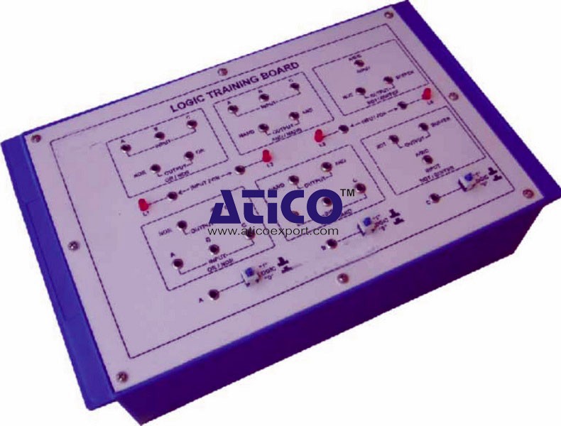
Features: The board consists of the following built-in parts...
DV/DT Limitation Of SCRs:- The offered range is known for enhancing the Dv/Dt capability of SCRs to avoid false firing which may be disastrous in some applications. This range is also known f...
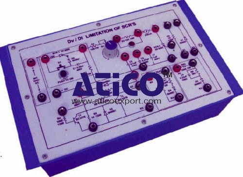
DV/DT Limitation Of SCRs:- The offered range is known for enhancing the Dv/Dt capability of SCRs to avoid false firing which may be disastrous in some applications. This range is also known for designing and studying various snubber circuits to improve the Dv/Dt capability of thyristors. Objects:
DV/DT Limitation Of SCRs:- The offered range is known for enhancing the Dv/Dt capability of SCRs to avoid false firing which may be disastrous in some applications. This range is also known for designing and studying various snubber circuits to improve the Dv/Dt capability of thyristors. Objects:
No Review Yet.
Features: The board consists of the following built-in parts...
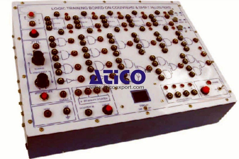
Features: The board consists of the following built-in parts...

Features: The board consists of the following built-in parts...
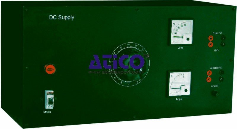
DC Supply is an important device in Electrical laboratories....
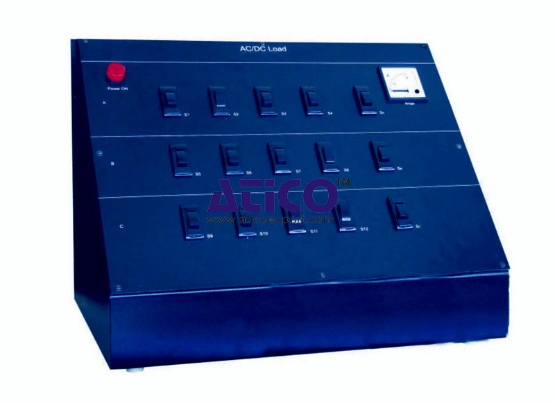
AC/DC Load is an important device in all the Electrical labo...
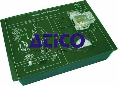
The Electrical Safety Demonstrator is a useful trainer for s...
Single Phase Transformer Lab is an elite training system for...
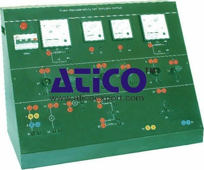
Power Measurement by Two Wattmeter Method Power Measurement...
Copyrights © 2026 All Rights Reserved by Atico

Product
Reviews
add Review
reviews
No Review Yet.